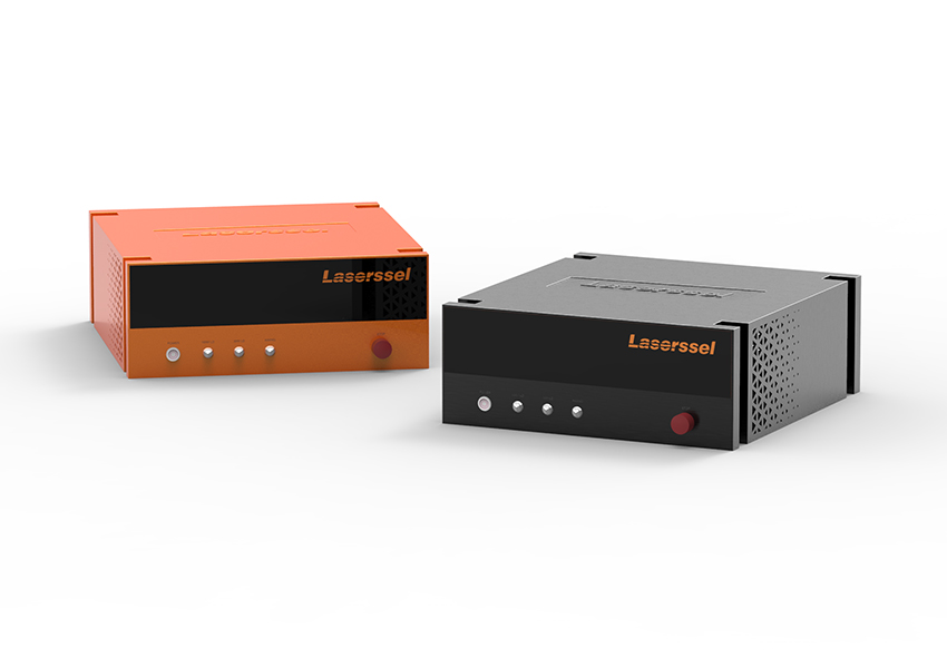
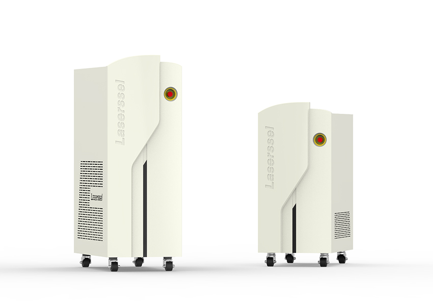
Laserssel, founded in 2015, is Laser based soldering and/or rework equipment manufacturer focusing on Semiconductor, Display and Automotive industries. The company provides Laser Selective Reflow (LSR) to above mentioned industries in number of different form factors.
Laserssel focuses on maximizing productivity in semiconductor back-end process, and solving thin die warpage issue commonly seen in ultra slim(~30um) die bonding and/or multiple die stack bonding such as HBM (High Bandwidth Memory). For this, we are prioritizing development of large area BSOM (Beam Shaping Optic Module) and high power Laser controller needed for large size BSOM. 12 kW Laser application and 80x240mm BSOM optimized for 80x240mm memory substrate is ready for launch beyond 100x100mm BSOM, and further targeting to develop BSOM for wafer level bonding.
In Display field, Laserssel uses small (100~200um beam size) Laser beam to rework defective LED from substrates of different kinds (FPCB, Glass, Rigid PCB, …). Recently display panels or backlight units using micro size LED (100um or even as small as 30um in dimension) are becoming popular for better brightness and/or vivid color representation on TV, Note PC or large size display. Approximately large number of LEDs are used for most advanced display products, 10K or more for backlight units and 1M or more RGB display and placing these LED chips and reworking defective units are becoming real homework for industry to solve. Laserssel has provided automated rework equipment that can rework – detach defective LED and replace with new LED – mini/micro LED placed on various substrates (FPCB, Glass, Al and others) in TV, Note PC, Tablet, Large size outdoor display applications.
Further, in automotive industry and other numerous SMT applications, Laser selective soldering has provided unique solution to reflow and/or rework BGAs and other smaller passive components such as capacitor and sensors on substrates, especially on thermally sensitive substrates or at position with very narrow gap to next adjacent components. European automotive makers have adopted Laser Selective Reflow for soldering sensor and capacitors on thermally sensitive FPCB for battery management system of electric vehicles.
Easy Engineering: A brief description of the company and its activities
LASERSSEL: As a pioneer in selective soldering segment, Laserssel has provided customers with unique soldering capabilities solving various problems in thin semiconductor package warpage enhancement, micro-sized LED component reflow / rework in advanced display and component bonding on thermally sensitive substrates and many other challenges that were difficult, if not impossible, in conventional reflow process.” Please walk us through this statement and shed some light on Solutions that you offer in the Semiconductor Tech Space on the basis of its methodology, features and benefits involved?
Laserssel has achieved acceptance from customers by solving problems that existing process and solutions had in various industries with LSR.
Warpage-free large size heterogeneous integration package bonding, mini LED rework and bonding small passive components on electrical vehicle battery FPCB are noteworthy examples.
In year 2018, customer was developing large size heterogeneous integration package of 60~70mm in size consisting of processor and memory. Issue with this development was to reflow two types of components with different thermal behaviours without warpage and good wetting on all bumps, which was difficult to achieve with existing technology, reflow oven or TC bonder. Laserssel was able to successfully bond this package without warpage or non-wet by reflowing with uniform Laser beam through large area BSOM for few seconds, and has supplied LSR to mass production process of this advanced semiconductor package, and continue to expand relationship with this customer today.
Mini LED Rework project was to rework 200um-size defect LED among 10,000 LEDs spacing 1mm apart each other on FPCB without damaging adjacent components and FPCB itself. Customer initially tried with hot air rework and spot Laser rework. Hot air rework failed to rework each component without affecting adjacent components, and spot Laser solution also failed because energy of spot Laser was too high not to damage FPCB near beam. Laserssel, however, was able to remove 200um size LED without damage to FPCB and reattach new LED with uniform Area Laser of hundreds micron size through BSOM.
Other significant achievement could be soldering small passive components on flexible PCB with LSR for BMS(Battery Management System) which controls current state of battery in electrical vehicle. Automotive industry, especially European premium electrical vehicle, tends to select non-flameable PEN(Polyethylene Naphtholate) material for BMS PCB that manages charging status of EV battery for battery combustion, ease of assembly and economic reason. PEN FPCB is non-flameable, but at the same time has low thermal resistance, meaning that it is not reflowable in conventional reflow oven.
For customers using PI material for battery PCB for its high heat resistance characteristics despite of its high cost, needs for selective reflow is increasing for attaching battery terminals at different soldering temperatures.
Laserssel’s LSR has already been adopted to number of European premium EV makers to solder components on thermally sensitive substrates with only few second of Laser emission without damaging FPCB or adjacent components.
E.E: What’s the news about new products?
LASERSSEL: Heterogeneous integration package, 80240 memory substrate reflow, stacked memory (HBM) bonding, SSD memory card module rework, 30um thin die bonding could be pointed out as key achievement, and some of them are described in previous questions.
80240 memory substrate reflow is to reflow traditional memory substrate with size 80x240mm with large BSOM with size 80x240mm for few seconds, and it can achieve extraordinary productivity compared to existing reflow oven.
SSD memory card rework is to rework defective NAND flash memory from SSD card. Key to this rework application is to rework target NAND chip while keeping temperature of adjacent location, hundreds micron apart, low enough not to damage other components.

E.E: What are the ranges of products?
LASERSSEL: LSR, in general terminology, refers to soldering equipment that uses Area Laser (homogeneous laser beam of required area (100x100um or 240x80mm or 100x100mm, …) with very high uniformity of energy density capable to reflow selected area on given substrate. With this principle, LSR ranges from reflowing large area substrates with one shot of Laser, bonding and reworking micro sized probe pins (10~20um size) on probe cards, small size LED rework and reflow on various substrates, reflowing very thin(50um) semiconductor die on PCB without warpage are all possible application of LSR.
E.E: At what stage is the market where you are currently active?
LASERSSEL: LSR is targeted to deliver solutions to niche market that existing mass reflow, thermal compression bonder, convection reflow cannot solve today. Laserssel sees most advanced semiconductor packaging with chip package size larger than 50x50mm, very thin die bonding (50um or thinner), very small component reflow/rework(mini/micro LED and AR/VR vision related products are facing difficulties in industry to find optimal and reliable reflow/rework solution and it can all become target market for Laser Selective Reflow.
E.E: What can you tell us about market trends?
LASERSSEL: Triggered by autonomous driving, IoT and rapidly increasing demand for data centre, demands for advanced semiconductor, high-performance AI chip and graphic processors, are dramatically increasing. These new technology demands innovative process skill to reflow packages such as large area heterogeneous integration package and/or ultra slim chip bonding without warpage.
Laserssel’s LSR(Laser Selective Reflow) equipped with large area BSOM has successfully provided solution for heterogeneous integration package bonding and currently in mass production. Also, LSR has dramatically improved productivity in ultra thin memory chip bonding without warpage and stacked die bonding with 4 or 8 stacks of thin die with one shot of Laser.
LSR is designed to shed Area Laser on carefully selected area for only few seconds without heating up surrounding area, eliminating concerns for damage to substrate or warpage issue.
E.E: What estimations do you have for the rest of 2022?
LASERSSEL: Laserssel is currently closing deals with numerous customers for year 2022 and discussing about 2023 projects now. I think 2021 has been setting ourselves as solution provider in number of different industries and 2022 has been year to penetrate into 2nd/3rd tier customers and expanding production capacity. I believe Laserssel now has solid reference and background in these field now and continuing to get new requests from new customers.
component reflow / rework in advanced display and component bonding on thermally sensitive substrates and many other challenges that were difficult, if not impossible, in conventional reflow process.” Please walk us through this statement and shed some light on Solutions that you offer in the Semiconductor Tech Space on the basis of its methodology, features and benefits involved?
E.E: What according to you are the distinct features of Laserssel /differentiating factors that give it a competitive edge?
LASERSSEL: Most significant feature of Laserssel technology would be technique to design uniform Area Laser with highly accurate optic technology and high-power Laser. Additionally, software controlling automated equipment and Laser recipe technique that was developed through numerous types of Semiconductor reflow experience could be said to be specialized competitiveness.
Laserssel strives to expand application area by solving various problems that customers face every day where existing solutions cannot handle in area such as advanced semiconductor packages, mini LED backlight units that has competitive edge in outdoor visibility and long lifetime and price competitiveness that are competing with OLED pre-dominating high-end display market and flexible PCBs that are not reflowable in high temperature conventional reflow oven or selective soldering area where different components soldering with different temperature profile is necessary, especially in rapidly growing electrical vehicle battery production industry where non-flameable flexible PCB reflow is required.
Semiconductor market, especially high performance AI chips and graphic processors, is explosively growing recently due to increased demands in autonomous driving, IoT and new Data Center construction. These high performance AI chips and graphic processors require very innovative design and production processes and existing reflow equipment cannot satisfy this new demands.
In the past, semiconductor front end technology has evolved to minimizing line width and 3nm line width has been developed up to today, but it is facing its limit to further reduce line width. ASML, front end equipment leader, commented in ASML Small Talk in 2021 that system improvements dominated by transistor scaling is saturating but 3 times enhancement every 2 years can still be achieved through advanced semiconductor packaging. TSMC also said in ISSCC 2021 roadmap presentation that realistically 50 billion transistors in one chip will be its development limitation, but in package level, it can be expanded 6 times to 300 billion transistors and they are currently in production.