Novel Crystal Technology (NCT) is a Japanese start up semiconductor company who focuses on Gallium Oxide (Ga2O3 ) for power devices. Ga2O3 power devices are expected to do high voltage power conversion efficiently with affordable pricing. They will gradually penetrate into market subsequently to Silicon Carbide (SiC) and Gallium Nitride (GaN) in latter half of 2020’s and will be widely adopted in 2030’s.
Easy Engineering: A brief description of the company and its activities.
Novel Crystal Technology: Talking about ourselves, our headquarters is located in Saitama, about 1 hour driving from downtown Tokyo, and we have around 80 employees. We spun off from Tamura Corporation in 2015 and have provided more than 460 researchers around the world with high quality substrates and epi wafers. We are also developing power devices by ourselves to prove the potential of the Ga2O3 semiconductor. We are fully dedicated to Gallium Oxide.
E.E: What are the main areas of activity of the company?
Novel Crystal Technology: We are working in the Power Electronics market. Ga2O3 gets attention in the market as the 3rd Wide Band Gap semiconductor, following SiC and GaN. Ga2O3 semiconductor is still in its infancy and no commercial power device is available yet. However, when we think about material’s properties, high efficiency due to low On Resistance while withstanding high voltage, HV applications such as Wind, Grid and Train will be the first areas where Ga2O3 power devices to be adopted.
For power device development, currently we are finding ideal edge termination structures to free up material’s Critical Electric Field (EC) characteristics. Although we have not completed this development, we already confirmed better EC value than SiC’s with our test chips this year. We will apply this expertise to our power device products to reduce power losses in HV applications. Ga2O3 semiconductor also draws attention from Automotive and Tier 1 manufactures whom currently increasing usage of SiC power devices. They expect future cost reduction. The bulk crystal of Ga2O3 is made from melt and its growth speed is much faster than SiC’s vapor growth. It will lead to significant difference in cost of substrates, and we will fully capitalize on it for price differentiation.
E.E: What’s the news about new products?
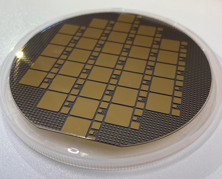
Novel Crystal Technology: We have 2 product lines. One is substrates and epi wafers, the other is power devices. Regarding epi wafers, we have launched our 3rd generation 100mm (4”) wafers last year and its quality has been greatly improved, for example, Killer Defect Density has become 10 times fewer than its previous generation. Also, we have started development of 150mm (6”) substrates last year. 150mm wafers are key products to penetrate into commercial power device market since most power device manufactures use 150mm fabrication lines. We plan to start initial production of 150mm epi wafers in late 2025. As for the power device products, we are developing 1200V Schottky Barrier Diode (SBD) with TO220 and 247 packages. Samples are under evaluation at some alpha customers and ES will be delivered in early 2024. We plan to start its production in 1st half of 2024 and the SBD will be the world’s first commercially available Ga2O3 power device.
E.E: What are the ranges of products?
Novel Crystal Technology: Currently, 2” and 100mm substrates and epi wafers are available with some orientation and doping substance options. They are mainly used for power device development. You can see brief products’ specifications at our website (www.novelcrystal.co.jp). About the power devices, we have samples of 1200V SBD now and plan to release next SBD products supporting wider voltage range, let’s say 650 ~ 3300V with much little reverse leakage current in late 2025.
E.E: At what stage is the market where you are currently active?
Novel Crystal Technology: Most of our customers are Universities and Institutes, so we are currently active in academia. However, some power device manufacturers and device users including our shareholders have worked on development and evaluation using our substrates and epi wafers. Recently, we got more inquiries from commercial market than before, therefore we are increasing our exposure in the commercial market from this year. We are expanding our active area from academia to commercial market.
E.E: What can you tell us about market trends?
Novel Crystal Technology: “From Lab to Fab”. We often hear this phrase recently, but it can be also applied to the Gallium Oxide semiconductor well. Some people pointed out that lack of p-type conductive layer is one of the critical disadvantages of practical Ga2O3 power devices. However, researchers from the U.S. and China recently announced encouraging R&D results one after another. They have developed Ga2O3 SBD test chips with heterogeneous materials for p-type conductors and those SBDs have shown significant Figure of Merit (FoM) in terms of breakdown voltage and efficiency. We are proud of their accomplishments as their epi wafer supplier. We expect to see positive responses from commercial power device manufactures in a few years. Ga2O3 power devices are leaving Lab soon.
E.E: What are the most innovative products marketed?
Novel Crystal Technology: I think the most innovative products is our material, Ga2O3 , itself. Our wafer products and device samples are still far behind from material’s theoretical properties. In other words, we have plenty of room for improvement, so we will continue our efforts to fully exploit material’s unprecedented potential. Therefore, we need some time to show you the most innovative our own products. And it can be applicable to you as well, because we license basic design data of our first SBD if you satisfy some of requirements. It means that you can develop your own SBDs based on the licensed design. You also have chances to develop the innovative products by yourselves.
E.E: What estimations do you have for 2023?
Novel Crystal Technology: Although most of our revenue comes from academia, we see strong demand this year and expect 25% revenue increase from last year. Regarding our R&D activities, we are working on some important projects both for wafers and power devices. We believe that we can share some good news with you around the end of this year, which tell you that commercialization of Ga2O3 semiconductor is upcoming. We expect that you will see more news about Ga2O3 in 2023 and hope that you feel familiar with Ga2O3 and NCT in due course.
Contact:
Novel Crystal Technology, Inc.
e-mail: sales@novelcrystal.co.jp
https://www.novelcrystal.co.jp/