POWATEC is a Swiss OEM specialized in the engineering and production of equipment related to the singulation of wafers and substrates in the semiconductor industry.
Easy Engineering: What are the main areas of activity of the company?
POWATEC: Our equipment includes Wafer Mounter, Wafer Laminator, UV-Curing System, Wafer Expansion, Film Frame, Cassette/Magazine and Accessories.
We serve Universities with lot size one to Fortune 1000 Companies with large production with our competence in manual and semi-automatic solutions. We use our own products in our Dicing Service facility. Our Dicing Service facility offers standard and customized dicing of all kinds of materials such as Silicon, Glass, FF4.
E.E: What are the ranges of products?
POWATEC: Our equipment is capable to process Wafers from 2” to 300mm diameter. We offer standard chucks and non-contact solutions. All our equipment requires a minimal footprint and offers high quality in clean room application at reasonable cost. POWATEC is known as a solution provider which customized the equipment to the specific needs.
In our dicing service we offer singulation of samples (lot size one) up to series production. We are ISO 9001 Certified.
E.E: At what stage is the market where you are currently active?
POWATEC: Our global presence has a history of 26 years. POWATEC is a spin-off from ESEC (former BESI) in Switzerland. Since then, POWATEC did focus on equipment around wafer dicing.

E.E: What can you tell us about market trends?
POWATEC: The semiconductor market especially for the equipment of production means is continuously growing. New technology trends such as the electrification, autonomous vehicles, 5G and many more require constant innovation in manufacturing methods. We expect that this trend will last for the upcoming decade.
E.E: What are the most innovative products marketed?
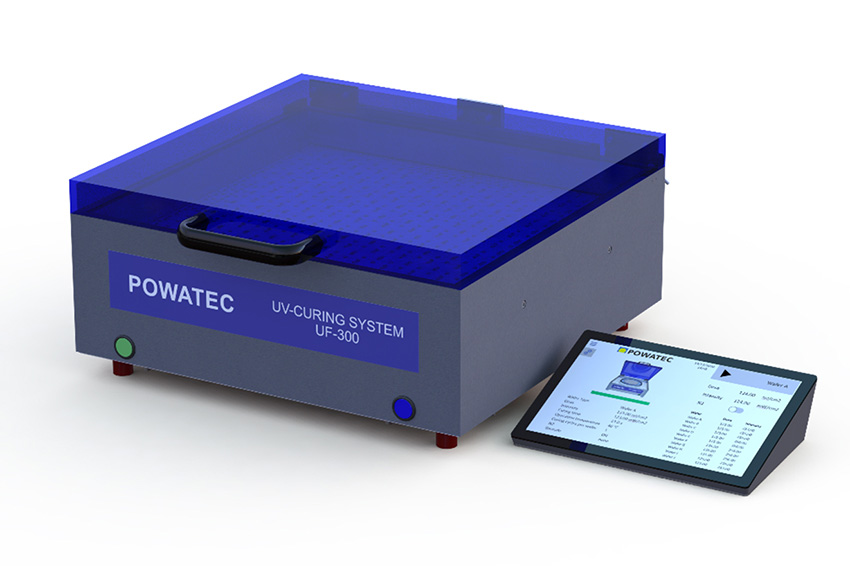
POWATEC: Our UF-300 UV curing system is the first fully SW controlled table-top device with 660 high performance UV LED’s. It fullfills highest requirements in quality control, precision and efficiency in clean room application and can be integrated into larger Semiconductor Equipment such as dicing saws or front end production machines (e.g. hybrid bonding).
On the other hand, POWATEC is developing a fully contact less vaccum mounter solution with a footprint of just 322 x 522 x 900mm. The Wafer is only in contact on 1mm of the border of the Wafer and kept in vacuum during mounting. No adjustments are necessary for different wafer thickness. All type of tapes can be used and immediately be exchanged.
E.E: What estimations do you have for 2022?
POWATEC: POWATEC is expecting the YoY growth in the Semiconductor Industry to continue for many more years to come. Additionally, leading Countries are investing billions in chip fabrication facilities to reduce their dependency of microchips from overseas productions. Another trend seems to contribute to the growth which is the fact, that the microchip and sensor production starts to be profitable at lower production volumes which allows small and mid caps to enter the market with innovative products.