Innoscience Technology, the company founded to create a global energy ecosystem based on high-performance, low-cost, gallium-nitride-on-silicon (GaN-on-Si) power solutions, has announced a new range of low voltage discrete HEMTs in FCQFN packaging. Rated at 40 V, 100 V and 150 V, the ‘flip chip’ formatting makes it simple for engineers to use.
Dr. Denis Marcon, General Manager, Innoscience Europe, comments: “We still also offer all our discrete devices in wafer scale packages which are beneficial for some module users, however the new FCQFN devices are easy to mount on PCBs using standard assembly equipment and processes.”
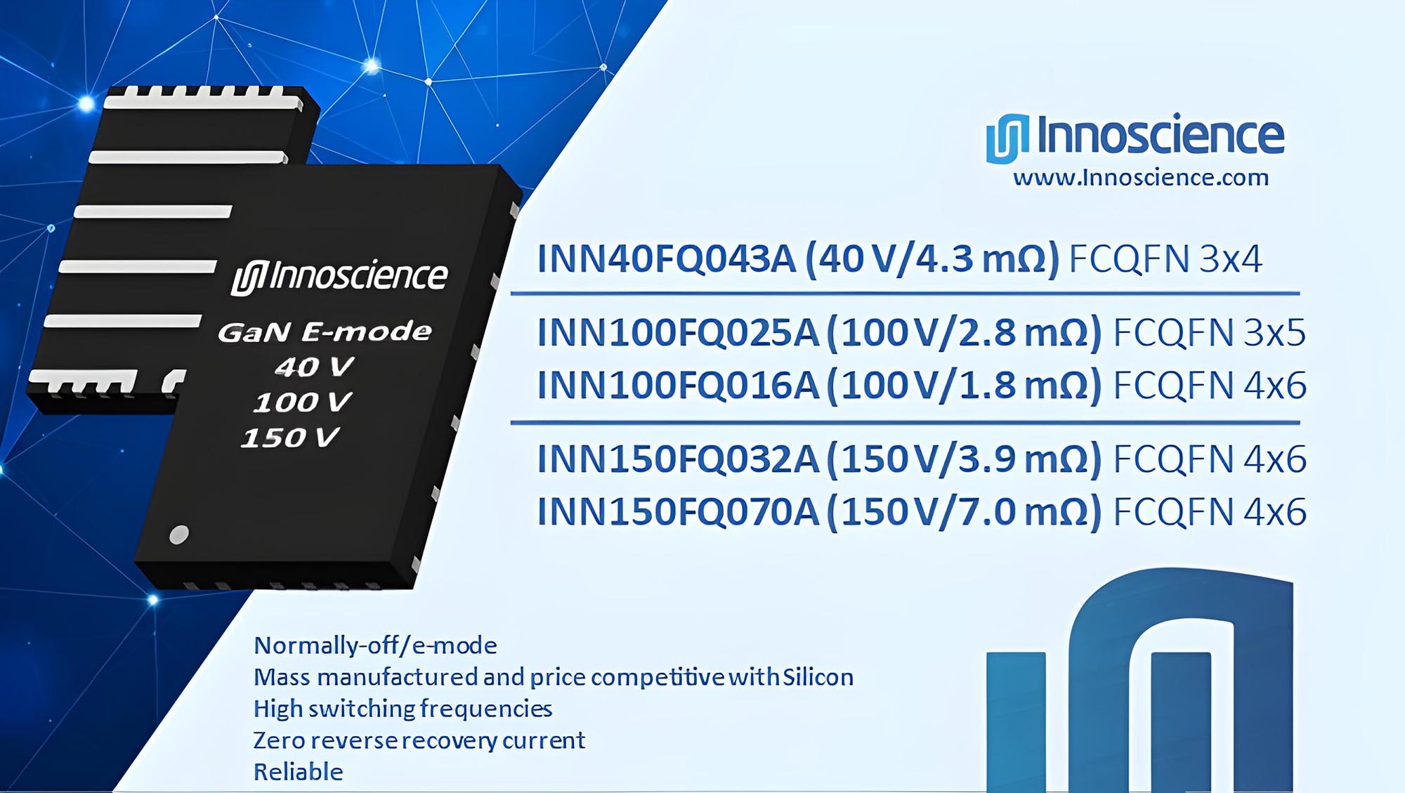
40 V-rated FCQFN devices are available with an on-resistance value of 4.3 mΩ (3×4 mm chip size). 100 V HEMTs are offered with RDS(on) ratings of 2.8 mΩ (3×5 mm) and 1.8 mΩ (4×6 mm), while the 150 V-rated parts measuring 4×6 mm are available with 3.9 mΩ and 7 mΩ RDS(on).
The 40 V parts using Innoscience’s latest GaN processes achieve industry-leading performance with best-in-class figure-of-merit (FOM) values for Qgg*Ron and Idss*Ron.
The parts low drain and gate leakage currents enable them to be used in mobile markets and direct-battery-connected applications. Other applications include USB Type C buck-boost converters in laptops. Furthermore, with its latest generation process, Innoscience maintains very tight control of the epitaxy, resulting in a very uniform threshold voltage and on-resistance, leading to a very high wafer yield.
100 V devices suit DC/DC conversion at power levels of up to 2 kW, due to their very low on-resistance. When used in parallel configuration, power levels up to 8 kW can be achieved.
The new 150 V targets industrial applications, including solar installations. They have been designed to be very rugged so they do not need the industry-standard 80% derating to be applied (i.e. they are rated at 100% of their voltage). All the new 40 V, 100 V and 150 V HEMTs have been tested to and exceeded JEDEC and the GaN-specific JEP 180 standards.
One last important point to highlight is that the 1.8 mΩ 100 V HEMTs are pin-for-pin compatible with the new 3.9 mΩ and 7 mΩ 150 V parts as they are all packaged in FCQFN 4x6mm: this enables great design flexibility.